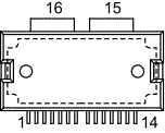
BLM7G22S-60PBG
Download datasheetThis device has been transferred from Ampleon to Flip Electronics.
BLM7G22S-60PBG
Download datasheetThis device has been transferred from Ampleon to Flip Electronics.
LDMOS 2-stage power MMIC
The BLM7G22S-60PB(G) is a dual path 2-stage power MMIC using Ampleon’s state of the art GEN7 LDMOS technology. This device is perfectly suited as general purpose driver in the frequency range from 2100 MHz to 2200 MHz. Available in gull wing or flat lead outline.
Features and benefits
- Integrated temperature compensated bias
- Biasing of individual stages is externally accessible
- Integrated current sense
- Integrated ESD protection
- Excellent thermal stability
- High power gain
- On-chip matching for ease of use (input matched to 50 Ω)
- Designed for broadband operation (2100 MHz to 2200 MHz)
- Compliant to Directive 2002/95/EC, regarding RoHS
Applications
- RF power MMIC for W-CDMA base stations 2100 MHz - 2200 MHz
Parametrics
| Symbol | Parameter | Conditions | Min | Typ/Nom | Max | Unit |
|---|---|---|---|---|---|---|
| frange | frequency range | 2100 | 2200 | MHz | ||
| PL(3dB) | nominal output power at 3 dB gain compression | 60 | W | |||
| Test signal: 2-c W-CDMA | ||||||
| Gp | power gain | PL(AV) = 1.6 W; VDS = 28 V | 29.5 | 31.5 | 33.5 | dB |
| RLin | input return loss | PL(AV) = 1.6 W; VDS = 28 V; IDq = 75 mA; IDq2 = 233 mA | -17 | -10 | dB | |
| ηD | drain efficiency | VDS = 28 V; f = 2140 Hz; IDq1 = 75 mA | 10 | 11.3 | % | |
| ACPR | adjacent channel power ratio | PL(AV) = 1.6 W; VDS = 28 V; f = 2140 Hz; IDq = 75 mA; IDq2 = 233 mA | -43 | -40 | dBc | |
Package / Packing
| Type number | Package | Outline version | Packing | Product status | Marking |
Orderable part number, (Ordering code (12NC)) |
|---|---|---|---|---|---|---|
| BLM7G22S-60PBG | OMP-780 (SOT1212-2) |
sot1212-2_po | Reel 13" Q1/T1 in Drypack | Transferred | Standard Marking |
BLM7G22S-60PBGY (9340 660 83518) |
Pinning info
| Pin | Symbol | Description | Simplified outline | Graphic symbol |
|---|---|---|---|---|
| 1 | VDS(A1) | drain-source voltage of stage A1 |

|
|
| 2 | VGSS(A2) | gate sense FET and gate source voltage of stage A2 | ||
| 3 | VDSS(A2) | drain sense FET source voltage of stage A2 | ||
| 4 | RF_IN_A | RF input path A | ||
| 5 | VGSS(A1) | gate sense FET and gate source voltage of stage A1 | ||
| 6 | VDSS(A1) | drain sense FET source voltage of stage A1 | ||
| 7 | n.c. | not connected | ||
| 8 | n.c. | not connected | ||
| 9 | VDSS(B1) | drain sense FET source voltage of stage B1 | ||
| 10 | VGSS(B1) | gate sense FET and gate source voltage of stage B1 | ||
| 11 | RF_IN_B | RF input path of B | ||
| 12 | VDSS(B2) | drain sense FET source voltage of stage B2 | ||
| 13 | VGSS(B2) | gate sense FET and gate source voltage of stage B2 | ||
| 14 | VDS(B1) | drain-source voltage of stage B1 | ||
| 15 | RF_OUT_A/VDS(A2) | RF output path A / drain source voltage of stage A2 | ||
| 16 | RF_OUT_B/VDS(B2) | RF output path B / drain source voltage of stage B2 | ||
| 17 | GND | RF ground |
Documentation
| Title | Type | Date | |
|---|---|---|---|
| Mounting and soldering of RF transistors in overmolded plastic packages | Application note | 2025-02-03 | |
| LDMOS 2-stage power MMIC | Data sheet | 2015-12-07 | |
| Packages for RF power transistors | Leaflet | 2024-10-25 | |
| RF power solutions for Wireless Infrastructure | Brochure | 2025-04-17 |
Design support
| Title | Type | Date | |
|---|---|---|---|
| Printed-Circuit Board (PCB) BLM7G22S-60PB(G) (Data sheet) | Design support | 2012-12-13 |