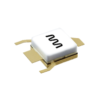
BLD6G21LS-50
Download datasheetTD-SCDMA 2010 MHz to 2025 MHz fully integrated Doherty transistor
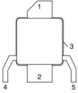
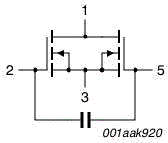
The BLD6G21L-50 and BLD6G21LS-50 incorporate a fully integrated Doherty solution using Ampleon’s state of the art GEN6 LDMOS technology. This device is perfectly suited for TD-SCDMA base station applications at frequencies from 2010 MHz to 2025 MHz. The main and peak device, input splitter and output combiner are integrated in a single package. This package consists of one gate and drain lead and two extra leads of which one is used for biasing the peak amplifier and the other is not connected. It only requires the proper input/output match and bias setting as with a normal class-AB transistor.
Features and benefits
- Fully optimized integrated Doherty concept
- Integrated assymetrical power splitter at input
- Integrated power combiner
- Peak biasing down to 0 V
- Low junction temperature
- High efficiency
- 100 % peak power tested for guaranteed output power capability
- Integrated ESD protection
- Good pair match (main and peak on the same chip)
- Independent control of main and peak bias
- Internally matched for ease of use
- Excellent ruggedness
- Compliant to Directive 2002/95/EC, regarding Restriction of Hazardous Substances
Applications
- High efficiency RF power amplifiers for TD-SCDMA multicarrier applications.
Parametrics
| Symbol | Parameter | Conditions | Min | Typ/Nom | Max | Unit |
|---|---|---|---|---|---|---|
| frange | frequency range | 2010 | 2025 | MHz | ||
| PL(3dB) | nominal output power at 3 dB gain compression | 50 | W | |||
| Test signal: TD-SCDMA | ||||||
| Gp | power gain | PL(AV) = 8 W; VDS = 28 V [0] | 13 | 14.5 | dB | |
| RLin | input return loss | PL(AV) = 8 W; VDS = 28 V; IDq = 170 mA [0] | -23 | -8 | dB | |
| ηD | drain efficiency | PL(AV) = 8 W; VDS = 28 V; 2010 MHz ≤ f ≤ 2025 MHz; IDq = 170 mA [0] | 39 | 43 | % | |
| PL(AV) | average output power | VDS = 28 V [0] | 8 | W | ||
| ACPR | adjacent channel power ratio | PL(AV) = 8 W; VDS = 28 V; 2010 MHz ≤ f ≤ 2025 MHz; IDq = 170 mA [0] | -24 | -20 | dB | |
| PARO | output peak-to-average ratio | PL(AV) = 8 W [0] | 9.4 | dB | ||
Package / Packing
All type numbers in the table below are discontinued.
| Type number | Package | Outline version | Packing | Product status | Marking |
Orderable part number, (Ordering code (12NC)) |
|---|---|---|---|---|---|---|
| BLD6G21LS-50 | ACC-400 (SOT1130B) |
sot1130b_po | Bulk Pack | Withdrawn | Standard Marking |
BLD6G21LS-50,112 (9340 635 09112) |
Discontinuation information
Pinning info
| Pin | Symbol | Description | Simplified outline | Graphic symbol |
|---|---|---|---|---|
| 1 | D | drain |

|

|
| 2 | G+BM | gate + bias main | ||
| 3 | S | source | ||
| 4 | n.c. | no connection | ||
| 5 | BP | bias peak |
Documentation
| Title | Type | Date | |
|---|---|---|---|
| TD-SCDMA 2010 MHz to 2025 MHz fully integrated Doherty transistor | Data sheet | 2015-12-07 | |
| Mounting and soldering of RF transistors in air cavity packages | Application note | 2025-02-03 | |
| Packages for RF power transistors | Leaflet | 2024-10-25 | |
| RF power solutions for Wireless Infrastructure | Brochure | 2025-04-17 |
No documentation available.