BLM2425M7S60P
Download datasheetBLM2425M7S60P
Download datasheetLDMOS 2-stage power MMIC
60 W dual path, 2-stage power MMIC transistor for Industrial, Scientific and Medical (ISM) applications at frequencies from 2400 MHz to 2500 MHz.
The BLM2425M7S60P is designed for high power CW applications and is assembled in a high performance plastic package.
Features and benefits
- High efficiency
- High power gain
- Excellent ruggedness
- Excellent thermal stability
- Integrated ESD protection
- Biasing of individual stages is externally accessible
- On-chip matching for ease of use
- Designed for broadband operation (frequency 2400 MHz to 2500 MHz)
- For RoHS compliance see the product details on the Ampleon website
Applications
- Industrial, scientific and medical applications in the frequency range 2400 MHz to 2500 MHz.
Parametrics
| Symbol | Parameter | Conditions | Min | Typ/Nom | Max | Unit |
|---|---|---|---|---|---|---|
| frange | frequency range | 2400 | 2500 | MHz | ||
| PL(1dB) | nominal output power at 1 dB gain compression | 60 | W | |||
| Test signal: CW class-AB @ 2450 MHz | ||||||
| Gp | power gain | PL = 30 W; VDS = 32 V [0] | 27.5 | dB | ||
| ηD | drain efficiency | PL = 30 W; VDS = 32 V [0] | 45 | % | ||
| PL(AV) | average output power | VDS = 32 V [0] | 60 | W | ||
Package / Packing
| Type number | Package | Outline version | Packing | Product status | Marking |
Orderable part number, (Ordering code (12NC)) |
|---|---|---|---|---|---|---|
| BLM2425M7S60P | OMP-780 (SOT1211-3) |
sot1211-3_po | Reel 13" Q1/T1 in Drypack | Active | Standard Marking |
BLM2425M7S60PY (9340 691 83518) |
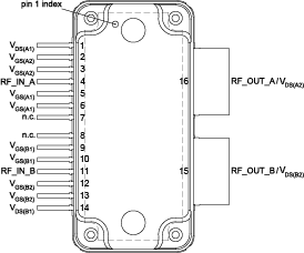
Pinning info
| Pin | Symbol | Description | Simplified outline | Graphic symbol |
|---|---|---|---|---|
| 1 | VDS(A1) | drain-source voltage of stage A1 |

|
|
| 2 | VGS(A2) | gate source voltage of stage A2 | ||
| 3 | VGS(A2) | gate source voltage of stage A2 | ||
| 4 | RF_IN_A | RF input path A | ||
| 5 | VGS(A1) | gate-source voltage of stage A1 | ||
| 6 | VGS(A1) | gate-source voltage of stage A1 | ||
| 7 | n.c. | not connected | ||
| 8 | n.c. | not connected | ||
| 9 | VGS(B1) | gate-source voltage of stage B1 | ||
| 10 | VGS(B1) | gate-source voltage of stage B1 | ||
| 11 | RF_IN_B | RF input path of B | ||
| 12 | VGS(B2) | gate-source voltage of stage B2 | ||
| 13 | VGS(B2) | gate-source voltage of stage B2 | ||
| 14 | VDS(B1) | drain-source voltage of stage B1 | ||
| 15 | RF_OUT_B/VDS(B2) | RF output section B / drain source voltage of stage B2 | ||
| 16 | RF_OUT_A/VDS(A2) | RF output section A / drain source voltage of stage A2 | ||
| flange | GND | RF ground |
Ordering & availability
| Type number | Ordering code (12NC) | Orderable part number | Distributor | Buy online | Samples |
|---|---|---|---|---|---|
| BLM2425M7S60P | 9340 691 83518 | BLM2425M7S60PY | DigiKey | Buy | Request samples |
| RFMW | Buy | ||||
| Mouser | Buy |
Documentation
| Title | Type | Date | |
|---|---|---|---|
| Mounting and soldering of RF transistors in overmolded plastic packages | Application note | 2025-02-03 | |
| LDMOS 2-stage power MMIC | Data sheet | 2017-09-13 | |
| RF power solutions for ISM, broadcast, navigation and safety radio applications | Brochure | 2025-03-10 | |
| RF power application reports for ISM, broadcast, navigation and safety radio applications | Brochure | 2025-04-08 | |
| Packages for RF power transistors | Leaflet | 2024-10-25 |
Design support
| Title | Type | Date | |
|---|---|---|---|
| Printed-Circuit Board (PCB) BLM2425M7S60P (Data sheet) | Design support | 2018-10-17 | |
| BLM2425M7S60P Model for Cadence AWR Microwave Office® | Simulation model | 2023-01-23 | |
| BLM2425M7S60P Simulation Example for Cadence AWR Microwave Office® | Simulation model | 2023-01-23 | |
| BLM2425M7S60P Model for ADS (Keysight Advanced Design System) | Simulation model | 2023-05-23 |