B10G2327N55D
Download datasheetB10G2327N55D
Download datasheetLDMOS 2-stage integrated Doherty MMIC
The B10G2327N55D is a 2-stage fully integrated asymmetrical Doherty MMIC solution using Ampleon’s state of the art LDMOS technology. The carrier and peaking device, input splitter, output combiner and pre-match are integrated in a single package. This device is perfectly suited as general purpose driver or mMIMO final in the frequency range from 2300 MHz to 2700 MHz. Available in PQFN outline.
Features and benefits
- Integrated input splitter
- Integrated output combiner
- Source impedance 50 Ω
- Pre-matched output
- High efficiency by asymmetric Doherty design
- Designed for large RF and instantaneous bandwidth operation, covering frequency from 2300 MHz to 2700 MHz
- Independent control of carrier and peaking bias
- Integrated ESD protection
- High power gain
- For RoHS compliance see the product details on the Ampleon website
Applications
- RF power MMIC for multi-carrier and multi-standard GSM, W-CDMA and LTE base stations in the 2300 MHz to 2700 MHz frequency range
Parametrics
| Symbol | Parameter | Conditions | Min | Typ/Nom | Max | Unit |
|---|---|---|---|---|---|---|
| frange | frequency range | 2300 | 2700 | MHz | ||
| PL(3dB) | nominal output power at 3 dB gain compression | 55 | W | |||
| Test signal: Pulsed CW | ||||||
| VDS | drain-source voltage | [0] [1] | 28 | V | ||
| Gp | power gain | [0] [1] | 24.8 | 27.5 | 31.2 | dB |
| ηD | drain efficiency | PL = 8 W (39 dBm) [0] [1] | 35 | 43 | % | |
| ηD | drain efficiency | PL = PL(3dB) [0] [1] | 42 | 48 | % | |
| RLin | input return loss | [0] [1] | -10 | dB | ||
Package / Packing
| Type number | Package | Outline version | Packing | Product status | Marking |
Orderable part number, (Ordering code (12NC)) |
|---|---|---|---|---|---|---|
| B10G2327N55D | PQFN-8x8 (SOT1462-1) |
sot1462-1_po | TR13; 500-fold; 16 mm; dry pack | Active | Standard Marking |
B10G2327N55DZ (9349 605 86515) |
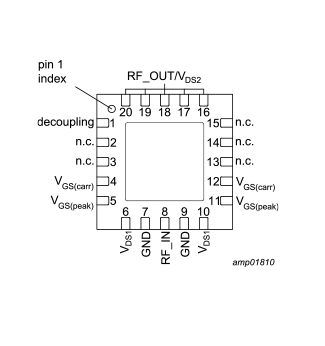
Pinning info
| Pin | Symbol | Description | Simplified outline | Graphic symbol |
|---|---|---|---|---|
| 1 | decoupling | video-lead for decoupling |

|
|
| 2 | n.c. | not connected | ||
| 3 | n.c. | not connected | ||
| 4 | VGS(carr) | gate-source voltage of carrier | ||
| 5 | VGS(peak) | gate-source voltage of peaking | ||
| 6 | VDS1 | drain-source voltage of driver stages | ||
| 7 | GND | RF ground | ||
| 8 | RF_IN | RF input | ||
| 9 | GND | RF ground | ||
| 10 | VDS1 | drain-source voltage of driver stages | ||
| 11 | VGS(peak) | gate-source voltage of peaking | ||
| 12 | VGS(carr) | gate-source voltage of carrier | ||
| 13 | n.c. | not connected | ||
| 14 | n.c. | not connected | ||
| 15 | n.c. | not connected | ||
| 16 | RF_OUT/VDS2 | RF output / drain-source voltage of final stages | ||
| 17 | RF_OUT/VDS2 | RF output / drain-source voltage of final stages | ||
| 18 | RF_OUT/VDS2 | RF output / drain-source voltage of final stages | ||
| 19 | RF_OUT/VDS2 | RF output / drain-source voltage of final stages | ||
| 20 | RF_OUT/VDS2 | RF output / drain-source voltage of final stages | ||
| flange | GND | RF ground |
Ordering & availability
| Type number | Ordering code (12NC) | Orderable part number | Distributor | Buy online | Samples |
|---|---|---|---|---|---|
| B10G2327N55D | 9349 605 86515 | B10G2327N55DZ | DigiKey | Buy | Request samples |
| RFMW | Buy | ||||
| Mouser | Buy |
Documentation
| Title | Type | Date | |
|---|---|---|---|
| LDMOS 2-stage integrated Doherty MMIC | Data sheet | 2022-11-11 | |
| Mounting and soldering of RF transistors in overmolded plastic packages | Application note | 2025-02-03 | |
| Packages for RF power transistors | Leaflet | 2024-10-25 | |
| RF power solutions for Wireless Infrastructure | Brochure | 2025-04-11 |
Design support
| Title | Type | Date | |
|---|---|---|---|
| Printed-Circuit Board (PCB) B10G2327N55D (Data sheet) | Design support | 2022-11-21 |